


Process
Porting
Process Porting Overview
Customer-provided data
- Process flow
- Cross-sectional structural diagrams
- Process conditions
- Material data
- Mask data
- Wafer data
Process development items
- Dimensions
- Film thickness
- Structure (depth/angle)
- Concentration profile
- Dimensional accuracy
- Defect information
- QC management methods
Provided by our company
- Process startup data
- PCM data
- Visual inspection result
- Wafer
Process Porting
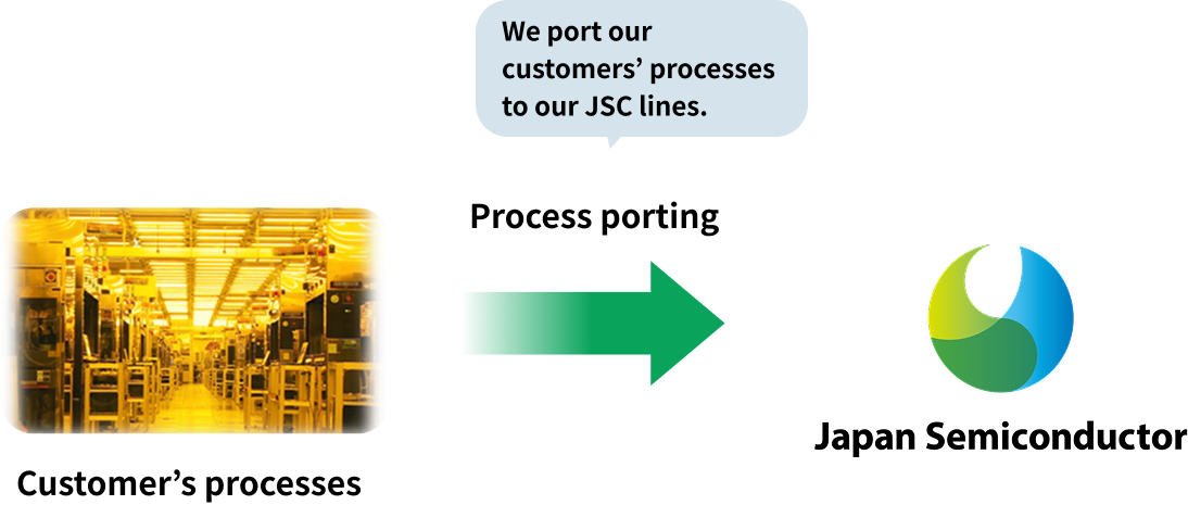
We transfer customers' processes to Japan Semiconductor's production lines for mass production.
Our Process Porting service transfers customers' processes to Japan Semiconductor's production lines.
Based on customer-provided information such as process flows, cross-section, process conditions, material information, mask information, and wafer information, we transfer your processes focusing on reproducibility and mass-production capability.
During the process transfer, we evaluate, review, and optimize process development items in-house, including dimensions, film thickness, structures (depth/angle), diffused dopant profiles, dimensional accuracy, defect information, and QC management methods.
Upon completion of the process transfer, we provide process startup data, PCM data, visual inspection results, and wafers, allowing customers to verify the startup status and quality on our production lines.