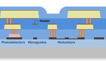
Silicon photonics
Using semiconductor manufacturing technology, we build optical circuits on wafers to achieve highly integrated optical devices.
Key Features
- Enables high-speed transmission, which is an advantage of optical communications.
- Can reduce environmental impact, by miniaturizing devices and lowering power consumption.
- Utilizing the 8-inch front-end process manufacturing mass production line, it allows prototyping and mass production in a Clean Room environment.
- Enables mask manufacturing and design support, process improvement and support for optical device performance, and process customization according to the customer’s requirements.
- We are working to reduce the manufacturing AT costs through an all-integrated system within Japan.