


Special process contracting
TSV(Through Silicon Via)
Since Toshiba started using TSV technology for volume production in 2007, we have met customer needs with high levels of quality and technical expertise.
* Part of the Back-end-process is handled in coordination with OSAT (outsourced semiconductor assembly and testing).
![[Image]: TSV (Through Silicon Via)](../../assets/img/foundry/en_wlcsp_img_02.png)
What Is the TSV (Through-Silicon Via) Process?
TSV (Through-Silicon Via) is a semiconductor manufacturing process that forms via interconnects passing through a Si wafer, enabling 3D integration and high-density packaging.
The entire process proceeds through wafer support (carrier attachment), → thinning → via formation → insulation → metal wiring → protective layer formation → solder ball mounting. The conditions of each process step directly affect electrical performance, reliability, and yield.
●Process Flow and Control Points
- Wafer Support: Glass attachment / glue thickness / glass / glue
First, a glass carrier attachment process is performed using glass as the carrier, to support the wafer through the glue of the adhesive layer. An important factor at this stage is the glue thickness, which affects the uniformity of the subsequent polishing process, and warping behavior. - Thinning: Back-side grinding / Si thickness
Next, we perform back-side grinding, which involves grinding and polishing the back side of the wafer, to thin it down to the desired Si thickness. The uniformity of the thinning process affects the exposure of the TSVs and the stability of wiring formation in subsequent processes. - TSV Formation: Via size top/Via size bottom/Via top/Min Via pitch
TSVs (Through-Silicon Vias) are formed after thinning. As design and process control metrics, we carefully manage Via size top (the dimension at the opening side), Via size bottom (the dimension at the bottom), Via top (the opening shape and edge condition), and Min Via pitch (minimum via pitch), which determines wiring density. These dimensions and shapes affect the quality of subsequent insulation layers and metal filling. - Insulation: CVD SiO₂
A CVD [chemical vapor deposition] SiO₂ insulating layer is formed on the via walls to ensure electrical isolation between the metal wiring and the Si substrate. Si film thickness and coverage affect leakage and reliability, it is important to optimize process conditions. - Metal Formation: Cu plating / Cu plating thickness / dimensions (L/S (Line and Space)) / M1 pad
Cu plating is used for vias and wiring. The thickness of the Cu plating determines the performance of the filling and wiring. If it is too thin, it can lead to increased resistance and the risk of voids, but if it is too thick, it can result in stress and poor flatness. When miniaturizing wiring, the dimensions (L/S (Line and Space)) of pattern design metrics are set appropriately, and if necessary, M1 pads are configured as connection pads. - Wiring and Protection: Cu wiring/Solder resist
After plating, the process moves on to wiring formation, where Cu wiring and solder resist are applied to protect the circuit and enhance assembly reliability. Design and process management for solder resist are crucial from the perspective of solder wetting and spread, as well as preventing solder bridges. - Mounting: Solder ball / solder ball mount
Finally, solder balls are formed as external connections, and the process is completed with solder ball mounting. Since ball diameter, placement position, and wettability affect assembly yield, these parameters are managed in conjunction with film quality, co-planarity, and resist conditions in upstream processes.
The TSV (Through-Silicon Via) process consists of multiple steps, from glass attachment to solder ball mounting. In particular, glue thickness, Si thickness, via top and bottom sizes, minimum via pitch, CVD SiO₂, Cu plating thickness, and dimensions (L/S (line and space)) are critical control parameters that determine product quality. We achieve stable mass production and high reliability by designing process conditions and monitoring with a focus on the interdependencies between processes, with awareness that inconsistencies in preceding processes lead directly to defects in subsequent processes.
●Features
- Reduces inter-chip wiring length by using through-Si vias
- Supports 3D and high-density packaging
- Balances performance and reliability by controlling glue thickness, silicon thickness, and via dimensions
- Low-resistance, high-reliability structures using SiO₂ insulation and Cu wiring
- Stable yield performance through process correlation management
●Main Applications
- CIS (CMOS image sensors)
- MEMS devices
- Advanced semiconductor packages requiring high density and reliability
WLCSP(Wafer Level Chip Scale Package)
We offer WCSP packages with TSVs.
Since Toshiba started using
TSV technology for volume production in 2007, we have met customer
needs with high levels of quality and technical expertise.
* Part of the Back-end-process is handled in coordination with OSAT (outsourced semiconductor assembly and testing).
Applications / TSV-based products
- CMOS Image Sensor; Consumer electronics, surveillance, automotive, medical, Line sensor and large-sized applications
- Si Interposer、Si-Package、Temporary bonding
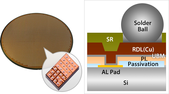
What Is WLCSP?
WLCSP (Wafer Level Chip Scale Package) is a semiconductor packaging technology that is fully integrated onto a Si wafer. This advanced packaging method enables ultra-compact packages that are roughly the same size as the chip itself.
In recent years, WLCSP has attracted attention as a technology that meets the demand for smaller size and higher performance in mobile and IoT devices.
WLCSP Structure
In WLCSP, redistribution starts from Al pads formed on the circuit on an Si substrate, through the passivation layer and the polyimide layer.
Optimizing terminal placement using an RDL (redistribution layer; Cu), and forming UBM (under-barrier metallization) on top of it, achieves stable connections with the solder balls.
In addition, SR (solder resist) ensures assembly reliability and durability.
Features
- Package size is almost the same as chip size; • RDL (Cu) allows high degree of freedom in terminal placement; • Excellent electrical properties due to shorter connections; • High mounting reliability, suitable for mobile and IoT applications
Main Applications
- PMICs, analog ICs, RF ICs, wearable devices, smartphones
- Widely adopted in applications requiring compact size and high-density packaging
RDL/Re-Distribution Layer
This technique facilitates bump formation and external connections by redistributing the electrode layout and relocating input/output terminals to optimized positions
![[Image]: RDL/Re-Distribution Layer](../../assets/img/foundry/foundry_special_img_01.png)
What Is RDL (Redistribution Layer)?
RDL (Redistribution Layer) is a core technology that enables electrode repositioning in WLP and Fan-Out packages. This semiconductor intermediate process technology eliminates I/O pitch constraints and enables high-density packaging by repositioning Al pad electrodes on a silicon substrate to locations suitable for external assembly.
The silicon surface is protected by a passivation layer, and only the Al pads are exposed.
We reposition the electrodes by forming a polyimide insulating layer and then fabricating Cu wiring on top of it as the RDL (Cu).
At this stage, UBM (under-barrier metallization) is applied directly beneath the RDL (Cu) to form the Cu wiring. It serves as a conductive substrate, acting as a seed layer to facilitate processes such as Cu plating. In addition, a layer is built in that ensures adhesion and prevents delamination at the interface between the polyimide and the metal. It also functions as a containment barrier to suppress the inter-migration of materials. With this layer configuration, RDL provides a wiring structure ideal for high-density packaging.
●Features
- Al pad electrodes are repositioned to eliminate I/O pitch constraints; • The polyimide insulation layer enables flexible and highly reliable wiring structures; • Adhesion of Cu plating to the seed layer for plating is ensured by UBM formation
- Improved long-term reliability through the diffusion barrier function
●Main Applications
- • WLP (Wafer-Level Package); • Fan-Out packaging; • Semiconductor packages for high-density pachaging; • Advanced devices requiring I/O redistribution
Cu Plating (with Au Top plating)
Due to the high conductivity and high reliability of Cu Plating (with Au Top plating), it supports multilayer wiring and thick-film wiring formation of semiconductor devices.
![[Image]: Cu Plating (with Au Top plating)](../../assets/img/foundry/en_foundry_special_img_02.png)
What Is Cu Plating (with Au Top Plating)?
Cu Plating (with Au Top Plating) is a semiconductor intermediate process technology in which Cu plating is formed on the substrate surface and Au Top plating is applied to the outermost layer.
Cu plating offers high electrical conductivity and the ability to form fine wiring, and is widely used in electronic components, semiconductors, and printed circuit boards.
Applying Au Top plating prevents Cu oxidation and improves corrosion resistance, solderability, and contact reliability.
●Features
- Cu plating enables low-resistance, high-conductivity wiring; • Au top plating improves corrosion resistance and contact reliability; • Excellent adhesion of the plating layer ensures long-term reliability
●Main Applications
- • Semiconductor packages; • Electronic components; • Modules; • Connectors and terminal components; • High-reliability printed circuit boards
Au Bump
The Au Bump process is a technique for forming fine bumps using gold (Au) to connect a semiconductor chip and circuit board with high reliability and high conductivity. It is ideal for high frequency, high-performance devices. The minimum processing size is 5 μm.
![[Image]: Au Bump](../../assets/img/foundry/foundry_special_img_03.png)
What Is Au Bump?
Au Bump is an electrode formation technology that supports highly reliable semiconductor devices. Au achieves uniform film thickness and excellent adhesion, making it suitable for fine-pitch flip-chip mounting.
Au bumps are fabricated via UBM on Al pads, improving electrical and mechanical reliability. Furthermore, precise control of passivation openings enables stable Au bump formation.
Au achieves stable electrical properties and assembly performance through diffusion barrier functionality and adhesion provided by UBM. It is widely adopted in LCD driver ICs and advanced semiconductor packaging.
●Features
- "• Uniform bump formation and support for fine pitch • Diffusion barrier functionality and high adhesion provided by UBM • Low contact resistance and excellent electrical and mechanical reliability"
●Main Applications
- • LCD driver ICs; • Flip-chip mounted devices; • Advanced semiconductor packages; • Electronic devices requiring high-reliability mounting
Color Filter
Color Filter (& Micro Lens) Technology
Toshiba boasts process technologies for color filters and microlenses for image sensors. We also provide consultation for product tuning, including the adjustment of sensitivity and spectral characteristics through mask tooling for color filters and microlenses.
Sensor cell size: 1.1 μm and greater
Color filter process: Red,
green and blue (RGB) + near infrared (NIR)
Your sensitivity and spectrum requirements are satisfied by adjusting the mask dimensions and the coating thickness.
Color filter structure / Microlens structure
Color filter structure
Sensitivity and cross points can be adjusted through the adjustment of color resist thickness and/or material selection. At your request, we will make a technical study.
![[Image]: Color filter structure](../../assets/img/foundry/en_colorfilter-structure_img_01.png)
Microlens structure
Microlenses are effective in improving light-harvesting performance. At your request, we will make a technical study for the adjustment of lens-to-lens gaps and microlens shapes.
![[Image]: Microlens structure](../../assets/img/foundry/en_colorfilter-structure_img_02.png)
What Is a Color Filter?
A color filter is a core technology used in image sensors. It separates light that is incident from a light source by wavelength, and accurately directs it to the photodiodes of each pixel.
In recent years, for image sensors, the mainstream design approach involves combining microlenses and color filters positioned on the pixels, to improve light-gathering efficiency and minimize the impact of inactive-area. Especially as cell pitch continues to shrink, it is important to optimize the design of large and small gaps between pixels. When gaps are large, inactive-area increase, leading to a decreased sensitivity. Conversely, in small gap structures, light interference with adjacent pixels is a challenge. In contrast, by optimizing the layout of color filters and the shapes of micro-lenses with crosspoints in mind, it is possible to suppress unwanted light leakage and achieve both accurate color reproduction and high signal quality. Furthermore, maximizing the light input efficiency to the photodiodes means that a high signal-to-noise ratio (S/N ratio) can be maintained even as the cell pitch is reduced. This delivers outstanding performance in industrial, automotive, and high-resolution imaging applications. The integrated optimization of color filters, inactive-area control, and gap design is key to achieving higher image quality in next-generation image sensors.
●Features
- • High-efficiency light collection to photodiodes through the combined use of microlenses
- • Color filter layout that minimizes inactive areas
- • Optimized gap design for fine pixel pitches
- • Excellent color reproduction and signal quality through cross-point optimization
- • High signal-to-noise (S/N) ratio maintained even at fine pixel pitches
●Main Applications
- High-resolution CMOS image sensors
- Automotive image sensors
- Industrial image sensors
- CMOS image sensors requiring compact size and high pixel density