


Analysis techniques of Us
Analysis techniques of JAPAN SEMICONDUCTOR CORPORATION
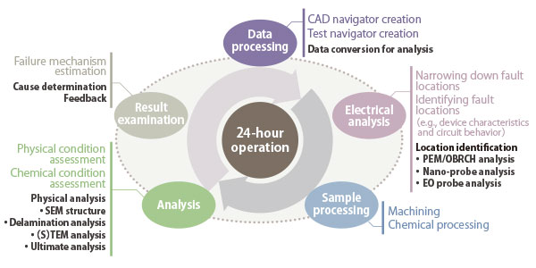
We have established a system that allows us to consistently carry out activities ranging from failure identification to physical analysis; we conduct physical analyses on a 24-hour basis and analysis results are used for failure mechanisms estimation.
Quality support system
We have been building trust through long-time business with major leading companies including top-ranked manufactures of automotive components (for engines and brakes).
- Response to complaints: First response within three days and final response within 10 days (TAT3/TAT10)
※The above response schedule is a target and actual response schedule is determined on a complaint-by-complaint basis. - Quality information/evaluation sample
- 1. We achieve just-in-time (JIT) delivery that satisfies your requirement based on an integrated system that involves our engineering, quality, and production sections.
- 2. We maintain enhanced assessment/analysis tools.
Failure analysis flow
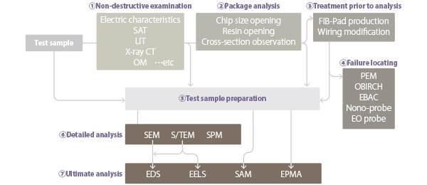
To identify the cause of the failure, we investigate the electric characteristics and carry out a non-destructive examination to fully understand the failure condition. Prior to analysis, we consider the best method.
Analysis techniques
1. Non-destructive examination
- SAT: Scanning acoustic tomograph
- A scanning acoustic tomograph is used to observe the inside of each package for delamination and cracks. In some cases, a reference product is used to make comparisons for determination (to check for delamination and voids).
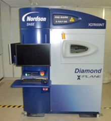
- X-ray CT: X-ray CT scanner
- An X-ray CT scanner is used to check packages for foreign matters between frames, bonding wire shape, paste wettability, and so on (check for abnormal wires and frames).
- TDR: Time domain reflectometer
- The electrodes of boards or packages that may be defective are probed and a fast pulse signal is input. Then, the reflected signal is observed for comparison with a non-defective product to check for defectives (open/short inside the board).
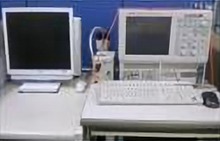
- LIT: Lock-in thermal emission analyzer
- With a signal input into a populated board or IC package, a thermal microscope is used to observe thermal emission from a defective location or locations (locate DC failures).
2. Failure locating techniques
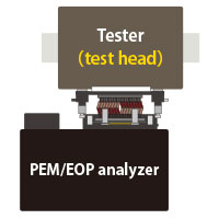
- Locating failures in a tester link
- With the product kept in operation, test heads are connected with a PEM/EOP analyzer to locate failures. As testers, two units of i-FLEX/T6573 are used. This method is available for wafers, packages, and individual chips.
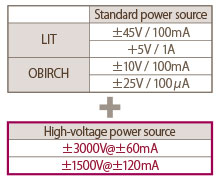
- High-voltage observation
- In addition to the standard power source, the OBIRCH/LIT equipment can use high-voltage power, allowing us to make observations at ± 750 V (safety measures taken).
3. Circuit modification/pad production service
FIB equipment can used to make circuit modifications, such as wiring connection and disconnection. In addition, we make a pad on passivation.
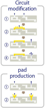
- Process
- 1. Exposing the wires to be connected
(using gas for insulator film milling) - 2. Connecting the two wires with each other
(Using conductor deposition gas) - 3. Exposing the wires to be disconnected
(using gas for insulator film milling) - 4. Disconnecting the exposed wires
(using gas for metal milling)
- 1. Exposing the wires to be connected
- Process
- 1. Exposing the desired wire
(using gas for insulator film milling) - 2. Embedding a conductor to form a pad
(Using conductor deposition gas)
- 1. Exposing the desired wire
- Supporting Cu wires and low-k films
- It is possible to process packages, wafers (6 and 8 inches), and chips.
- Navigation to the processing position based on CAD data (in GDSⅡ format)
- We can undertake integrated operations covering jobs ranging from pretreatments, such as IC package opening and polyimide separation, to FBI processing.
